
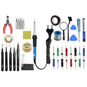
Key Characteristics & Benefits:
- Material: High-conductivity red copper.
- Diameter: Extremely thin (0.1mm or ~0.004 inches) for microscopic work.
- Insulation: Coated with a thin layer of insulation to prevent short-circuiting against other components.
- Direct Welding: Often can be soldered directly without removing the enamel.
- Flexibility: Easily pliable for routing on complex, dense PCBs (motherboards).
- Applications: Used for repairing fingerprints, IC pin connections, and broken traces in smartphones, laptops, and other electronics.
Reviews
There are no reviews yet.